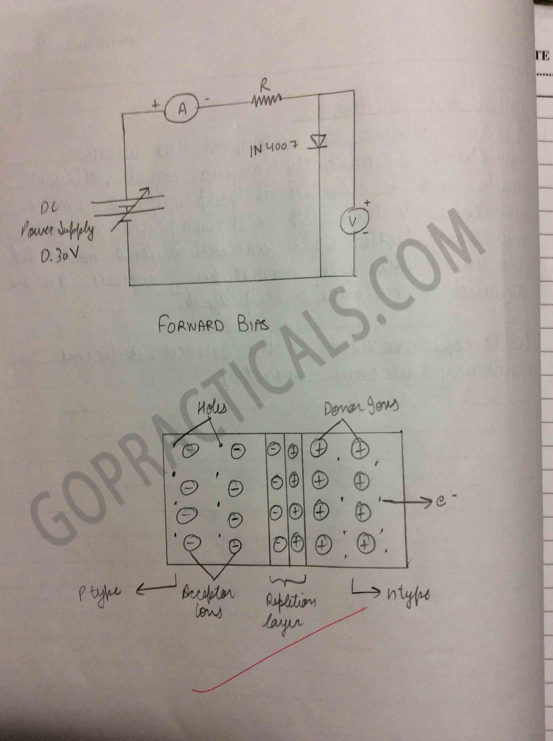
When P and N semiconductors are joined to make the PN junction semiconductor diode, the electrons near the PN junction jump from N to P and holes near the junction jump from P to N. This phenomenon creates a depletion layer.
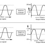
Do check out – Diode Application in Clamper Circuit
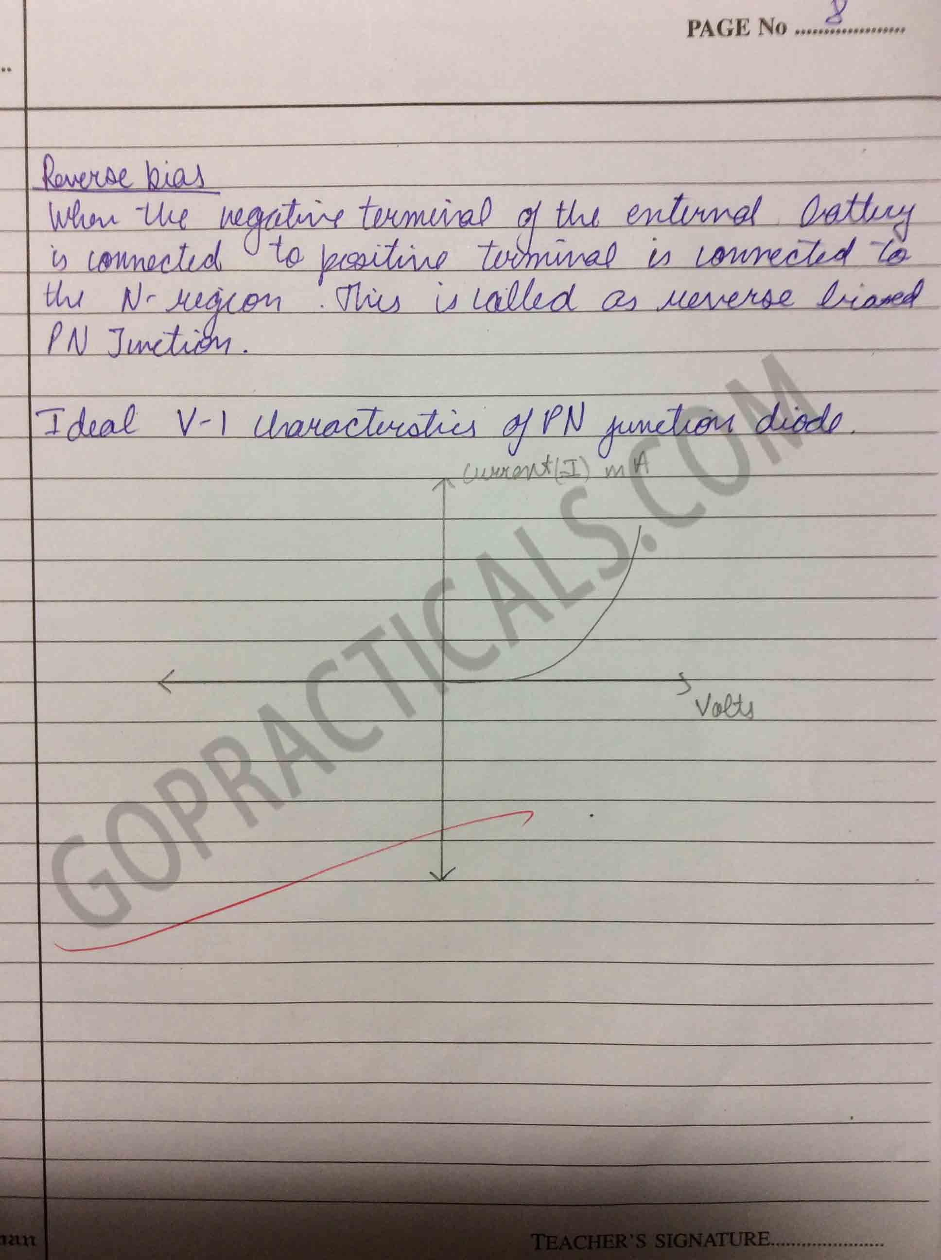
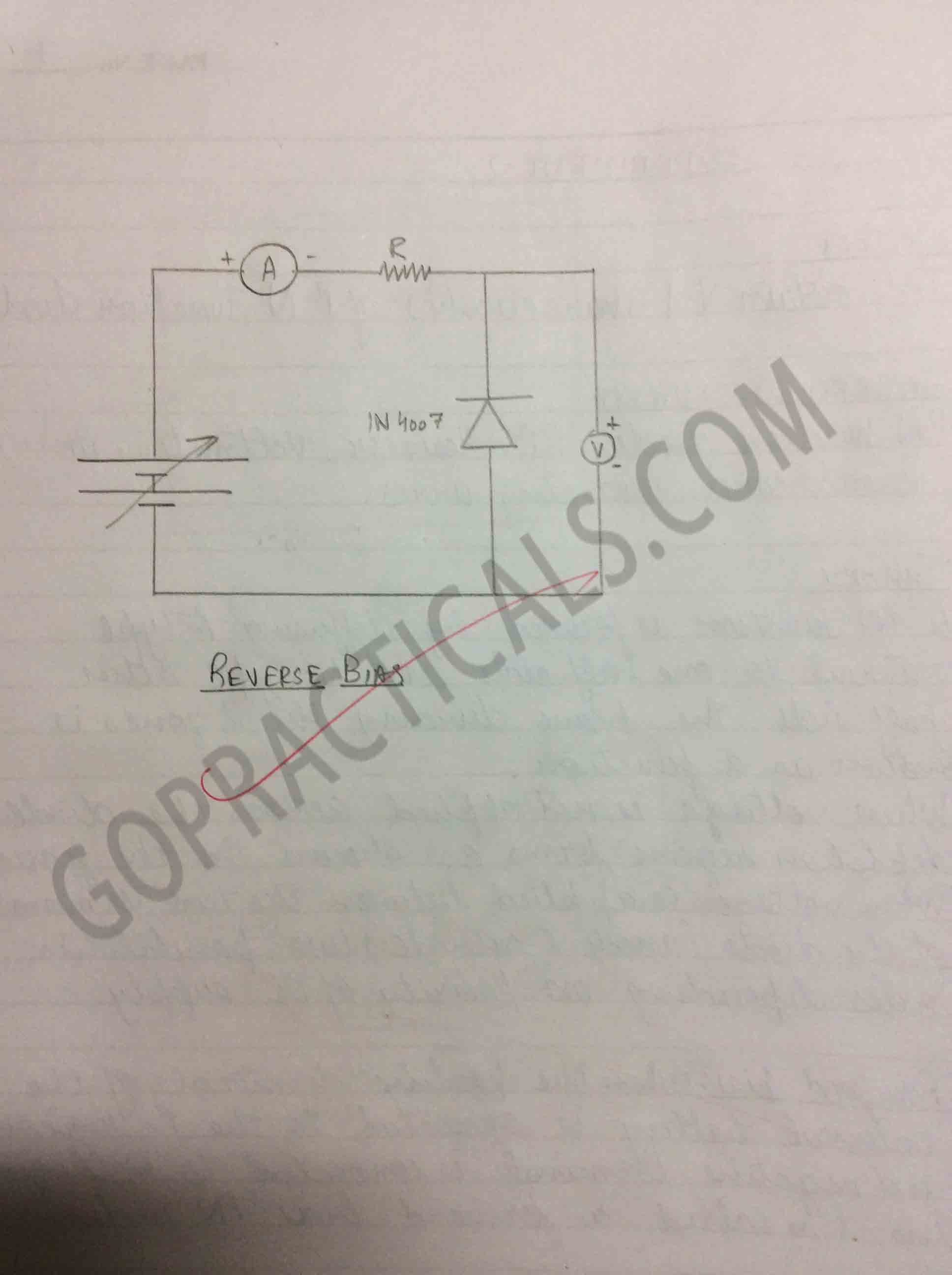
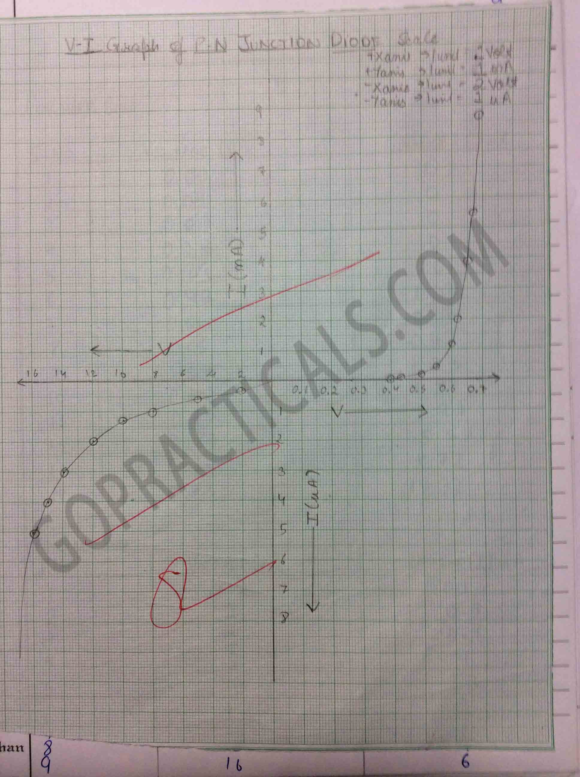
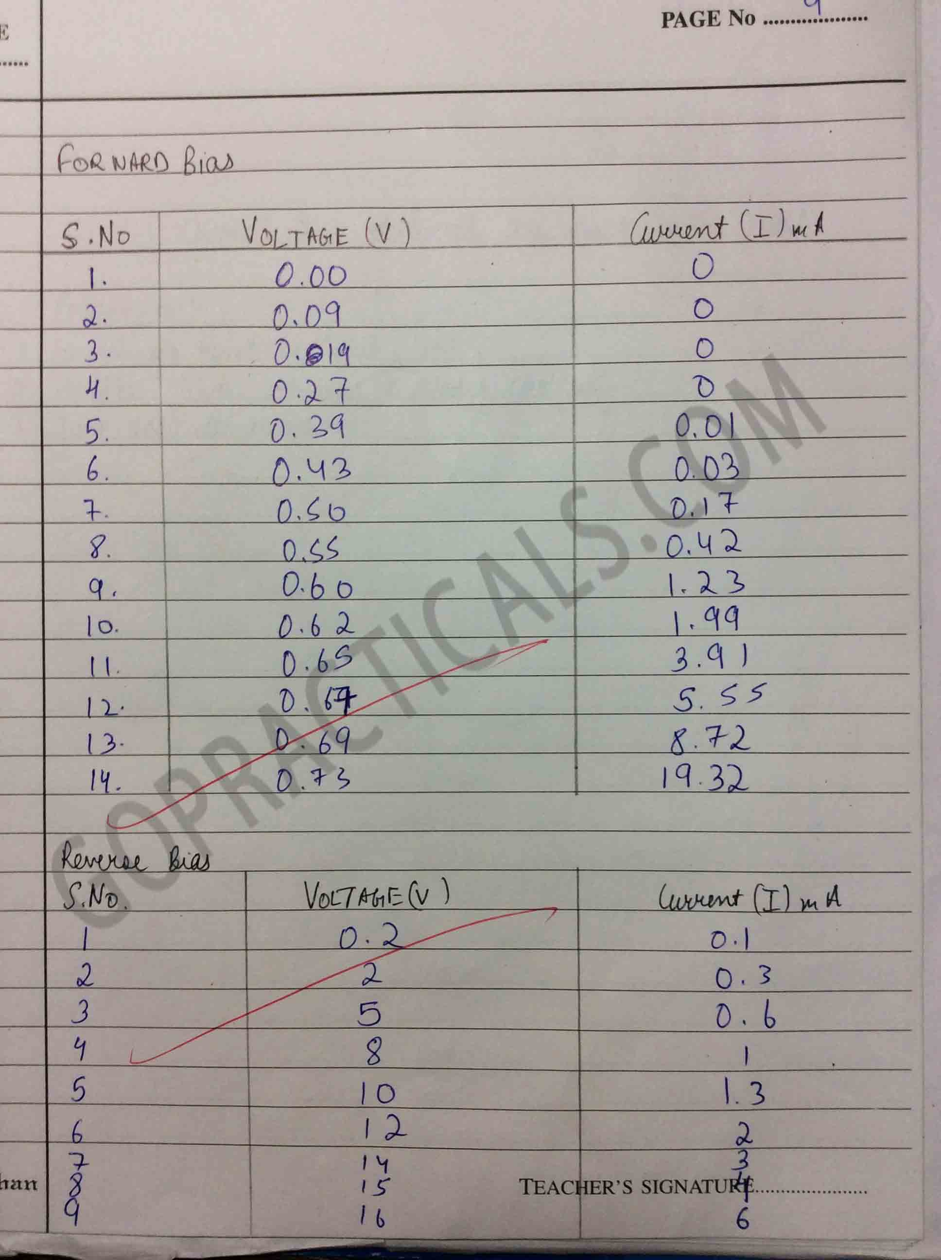
In this practical we will learn to obtain and draw the graph of V-I characteristic of a PN junction diode.
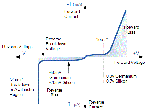
Practical on V-I characteristics of P-N Junction Diode

Watch this Video about the V-I characteristics of PN Junction Diode
>
Thanks for viewing our post, hope you liked it and do share our posts.
To obtain V-I characteristics of PN Junction Diode – Electronics Practical

